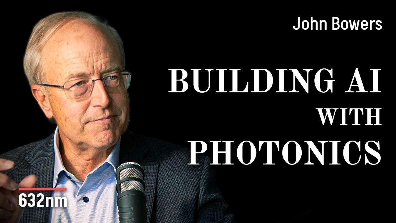
📺 Today’s recommended deep-dive video: https://www.youtube.com/watch?v=fjQ3Yorw-Ps
Lighting the Path for AI: How Silicon Photonics Reinvents the Data Center
As AI models balloon to require millions of processors, traditional copper interconnects are hitting a physical wall characterized by extreme heat and signal degradation. John Bowers, a pioneer in silicon photonics, explains how moving light directly onto the chip is no longer a luxury but a fundamental requirement for the next era of computing.
Core Question: How does integrating lasers directly onto silicon chips solve the scaling, power, and reliability bottlenecks of modern AI infrastructure?
Highlights
- The transition from copper to optical interconnects is necessary to overcome the 20 dB loss per meter seen at 100+ GHz speeds.
- Heterogeneous integration allows III-V materials to be bonded to silicon, providing the “gain” that silicon naturally lacks.
- Self-injection locking to high-Q resonators has enabled on-chip lasers to achieve ultra-narrow 1 Hz linewidths for precision metrology.
- Optical switching in data centers allows for instant redundancy, enabling the replacement of failed processor nodes without manual intervention.
⏱️ Reading time: approx. 10 minutes · Saves you about 89 minutes vs. watching.
Want to take notes while watching? Click the image below and let AI Notebook capture the key points for you 👇

The Copper Wall and the AI Imperative
The Death of Electrical Interconnects
We have reached a junction where copper traces can no longer keep pace with the 100 terabit switching chips powering modern AI.
At frequencies of 100 GHz and beyond, copper is incredibly inefficient; you might lose 20 dB of signal over just a single meter, necessitating power-hungry regeneration at every step. Light, by contrast, suffers the same negligible loss whether it travels a millimeter or a kilometer across a data center, making it the only viable medium for the “warehouse-scale computer” vision where millions of GPUs must act as a single unit.
The massive power density of modern racks, often reaching kilowatts of output, means that every picojoule per bit saved by switching to optics is a direct win for thermal management. If we cannot get the data off the chip without melting it, the evolution of AI simply stops.

💡 Digging Deeper
Q: Why is copper loss so severe now?
A: As clock speeds rise to support terabit chips, the capacitance and skin effect in copper lines require exponential power to drive signals, whereas photons require the same energy regardless of distance.
Q: How does this impact AI specifically?
A: AI models require massive clusters of processors to work in perfect synchronization; photonics allows these nodes to be spaced kilometers apart while maintaining the connectivity of a single rack.
Q: What is “OEO” switching?
A: It stands for Optical-Electronic-Optical, a process where light is converted back to electricity to be switched and then regenerated. It is expensive and slow compared to pure optical switching.
The Art of Heterogeneous Integration
Solving the Silicon Emission Problem
Silicon is the perfect material for waveguides and high-volume manufacturing, but its indirect bandgap makes it a “lousy” light emitter, producing only one photon for every million electrons.
To solve this, Bowers and his team pioneered heterogeneous integration, which involves bonding thin layers of III-V materials, like Indium Phosphide, directly onto 300mm silicon wafers. This creates a “best of both worlds” scenario: you get the high-efficiency gain of the III-V material with the extreme precision and scale of a standard CMOS foundry.
While foundries were initially conservative about introducing new materials, the maturation of these processes at places like Intel and Tower Semiconductor has led to the sale of over a billion dollars worth of heterogeneous transceivers.
💡 Digging Deeper
Q: How is the bonding actually performed?
A: An oxygen plasma activates the surfaces of both the III-V material and the silicon, allowing them to form a direct covalent bond that is robust enough for high-volume manufacturing.
Q: What happens if a portion of the wafer is defective?
A: Unlike monolithic growth, heterogeneous integration allows you to pre-inspect “chiplets” of gain material and only bond the known-good die to the silicon wafer, drastically improving yield.
Q: Why are Quantum Dots important here?
A: Quantum dots are insensitive to the dislocations that usually kill semiconductor lasers, and they are naturally reflection-immune, which eliminates the need for bulky optical isolators.
Precision Metrology on a Chip
From Megahertz to Millihertz
For decades, semiconductor lasers were viewed as “messy” and noisy compared to their gas or solid-state counterparts, typically limited to megahertz linewidths.
By self-injection locking a semiconductor laser to a high-Q silicon nitride spiral resonator, Bowers’ group has collapsed that noise floor, achieving linewidths as narrow as 1 Hz. This isn’t just a laboratory curiosity; it effectively puts the precision of a multi-million dollar metrology lab onto a chip the size of a fingernail.
This level of stability is the foundational requirement for next-generation optical clocks and autonomous navigation systems. If every vehicle has an inexpensive, chip-scale optical gyroscope and clock, we can achieve high-precision navigation even in GPS-denied environments.

💡 Digging Deeper
Q: What is self-injection locking?
A: It is a process where a tiny amount of light back-scatters from a high-Q resonator back into the laser, forcing the laser to adopt the resonator’s stable frequency and significantly reducing noise.
Q: How long is the cavity on these chips?
A: By using tight spirals in silicon nitride, researchers can pack up to four meters of optical path length into a square centimeter.
Q: Does this replace microwave clocks?
A: Yes, optical clocks are orders of magnitude more accurate than microwave ones; the challenge is shrinking them from table-top experiments to integrated circuits.
The Entrepreneurial Lab and Future Frontiers
Coaching the Next Generation
Bowers views the graduate school experience as a “hungry” period where students should tackle “stark and important” problems rather than safe, incremental ones.
He emphasizes that science is only useful if someone cares about the result, constantly asking his students: “Suppose you are completely successful—will it matter?” This philosophy has birthed numerous startups, moving technology from UCSB cleanrooms to global deployment in Google data centers.
Looking forward, the integration of AI into the design process itself—using “AI agents” to optimize chip layouts for power and area—promises to accelerate photonic development faster than human designers ever could.

💡 Digging Deeper
Q: What is the biggest mistake academic startups make?
A: Running out of money and lacking product focus; Bowers stresses that a CEO’s job is bringing in capital and defining specs, not just polishing the technology.
Q: Is optical computing finally happening?
A: It is finding a niche in vector-matrix multiplication for AI, but it struggles to compete with the general-purpose flexibility of traditional silicon CMOS.
Q: Why was the 2000-era optical switching boom a failure?
A: The technology was 20 years ahead of its time; the industry didn’t have the data volume or the reliability needs that today’s AI models finally demand.
Key Takeaways
The transition to silicon photonics is driven by a cold, physical reality: copper cannot scale to the speeds AI requires. By integrating lasers directly onto silicon, the industry gains the ability to move massive amounts of data with minimal heat, utilizing the same CMOS foundries that built the modern world. This represents a fundamental shift in computer architecture, moving from a collection of isolated boxes to a unified “warehouse computer” where light is the nervous system.
Beyond the data center, the ability to create ultra-stable, narrow-linewidth lasers on-chip opens the door to ubiquitous high-precision sensing. Whether it is LiDAR for every car, non-invasive glucose monitoring, or chip-scale atomic clocks for GPS-independent navigation, the convergence of III-V materials and silicon is transforming “lab-only” physics into mass-market consumer reality.
Finally, the success of these technologies relies on a combination of long-term research vision and aggressive productization. As John Bowers notes, the most impactful science is born when researchers stay “hungry” and focus on solving bottlenecks that prevent the next leap in human capability, supported by an ecosystem that values yield and reliability as much as a Nature paper.
Q&A
Q1: Why not just use all-silicon light sources instead of bonding III-V materials?
A: Silicon is an indirect bandgap material, making it roughly a million times less efficient at emitting light than III-V materials; it simply cannot provide the power levels needed for data centers.
Q2: What is the main advantage of co-packaged optics?
A: It places the photonics inside the same package as the GPU or switch chip, eliminating the long copper traces that cause massive signal loss and high power consumption.
Q3: How does optical switching improve data center reliability?
A: In a cluster of a million processors, units fail every day. Optical switches allow the system to electronically reroute data to a backup processor instantly, without needing a technician to physically swap a card.
Q4: Can these integrated lasers survive high temperatures?
A: Yes, by using silicon’s high thermal conductivity and advanced heat-sinking, these heterogeneous lasers can operate at temperatures as high as 150°C to 185°C.
Q5: What is a soliton in the context of frequency combs?
A: A soliton is a stable optical pulse that maintains its shape because the material’s nonlinearity perfectly balances its natural dispersion. In photonics, a train of these solitons creates a “comb” of perfectly spaced frequencies.
Q6: Why is 300mm wafer scale testing a “revolution”?
A: Traditional photonics required hours to test a single device. Silicon photonics allows an entire wafer to be characterized in a single shift, identifying good die before the expensive packaging process begins.
Q7: Will photonics ever replace electronic processors entirely?
A: Unlikely. Electronics are superior for general-purpose logic and memory, while photonics is unbeatable for interconnects and specific math tasks like vector-matrix multiplication. The future is a hybrid of both.