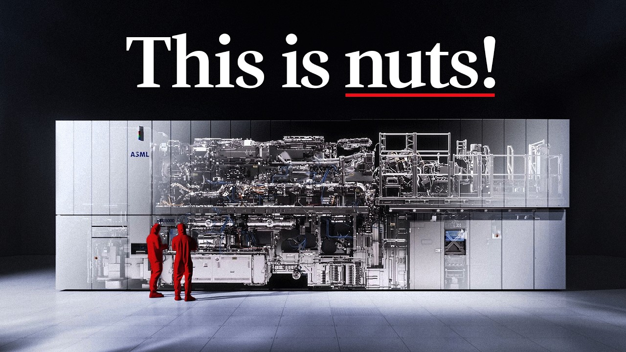
📺 Today’s recommended deep-dive video: https://www.youtube.com/watch?v=MiUHjLxm3V0
The Machine That Saved Moore’s Law: Inside ASML’s Impossible Engineering
For decades, the digital revolution relied on a simple promise of doubling transistor density every two years, but by 2015, the tech industry hit a physical wall that threatened to halt progress forever. This is the story of how a single company in the Netherlands spent thirty years and billions of dollars to build a machine so complex it was once dismissed as a “fish story.”
Core Question: How did ASML overcome the fundamental laws of physics to create Extreme Ultraviolet (EUV) lithography machines that print circuits at the atomic scale?
Highlights
- The physics of light: Why traditional lithography hit a “wavelength wall” at 193 nanometers.
- Artificial Suns: Using high-powered lasers to blast tin droplets 50,000 times per second to generate EUV light.
- Universal Smoothness: Mirror systems so perfect that if scaled to the size of Earth, their largest bump would be a millimeter high.
- The Unreasonable Gamble: How a global consortium of chipmakers saved the project after governments and competitors walked away.
⏱️ Reading time: approx. 8 minutes · Saves you about 47 minutes vs. watching.
Want to take notes while watching? Click the image below and let AI Notebook capture the key points for you 👇

The Crisis of Scale and the Rayleigh Limit
The Physics of Shrinking
For over fifty years, the number of transistors on a microchip doubled every two years, a trend known as Moore’s Law that drove the exponential growth of computing power. However, around 2015, the industry reached a breaking point where the light used to “print” these chips was simply too large for the features it needed to create.
This limitation is governed by the Rayleigh Equation, which states that the smallest feature you can print is determined by the wavelength of light and the size of the lens.
Traditional deep ultraviolet (DUV) machines reached their limit at a wavelength of 193 nanometers, leaving engineers with a choice: build infinitely large lenses or find a radically shorter wavelength. The solution was Extreme Ultraviolet (EUV) light, clocking in at a mere 13.5 nanometers, which promised to shrink transistors to the size of a few dozen atoms. But there was a catch: EUV light is so fragile that it is absorbed by almost everything, including the very air we breathe.

💡 Digging Deeper
Q: Why can’t we just use standard lenses for EUV light?
A: At 13.5 nanometers, light has enough energy to be absorbed by glass. Standard lenses would simply block the light instead of focusing it.
Q: What was the “brick wall” encountered in 2015?
A: It was the point where multi-patterning with DUV light became too expensive and physically imprecise to continue shrinking features reliably.
Q: Who first proposed using EUV?
A: Hiroo Kinoshita in Japan first demonstrated that x-rays could be bent using special mirrors in the 1980s, though he was initially laughed at by the scientific community.
Creating a Star in a Box: The EUV Source
The Tiny Supernova
Since EUV light doesn’t exist naturally in a usable form on Earth, ASML had to develop a way to create a tiny “sun” inside a vacuum chamber. The process is a masterpiece of precision violence that involves molten tin droplets the size of a white blood cell being shot through a chamber at 250 kilometers per hour.
A high-powered CO2 laser hits each of these droplets twice—first to flatten it into a “pancake” and then to vaporize it into a plasma that reaches 220,000 Kelvin.
This process happens 50,000 times every single second, creating a continuous stream of photons. The challenge isn’t just hitting the target; it is managing the debris, as stray tin atoms can instantly ruin the machine’s multi-million dollar optics. ASML engineers solved this by using a high-speed hurricane of hydrogen gas to catch the tin and flush it out as a gas called stannane, keeping the internal mirrors clean for up to a year of continuous operation.

💡 Digging Deeper
Q: How hot is the plasma created by the laser?
A: It is roughly 40 times hotter than the surface of the sun, reaching temperatures of over 220,000 Kelvin.
Q: Why use tin instead of xenon gas?
A: Tin has a much higher “conversion efficiency,” meaning more of the laser’s energy is turned into usable 13.5nm light compared to other materials.
Q: How do they ensure the laser never misses a droplet?
A: The machine uses a “nervous system” of laser curtains and sensors that track the position of every droplet in real-time to trigger the pulse at the exact microsecond.
The Smoothest Mirrors in the Universe
Precision Beyond Human Comprehension
Because EUV light is absorbed by glass, ASML and their partner Zeiss had to develop a system of mirrors that use “constructive interference” to reflect light rather than refract it. These mirrors are composed of roughly 40 to 100 alternating layers of silicon and molybdenum, each layer precisely tuned to a fraction of a wavelength.
These are likely the smoothest man-made objects in existence, polished to a degree where any bump is measured in the thickness of individual atoms.
To put this into perspective, if one of these mirrors were expanded to the size of the entire planet Earth, the largest deviation from its perfect curve would be no thicker than a single playing card. This level of perfection is non-negotiable because the light must bounce off six or more mirrors before hitting the wafer; even a tiny misalignment would cause the final pattern to be blurry or misplaced.

💡 Digging Deeper
Q: How accurate is the mirror’s pointing system?
A: It is measured in pico-radians. ASML uses the analogy of pointing a laser from Earth and hitting a dime on the surface of the moon.
Q: Why do they need so many layers of molybdenum and silicon?
A: Each single boundary only reflects a tiny fraction of light. By stacking dozens of layers, the reflections add up (interfere constructively) to reach about 70% reflectivity.
Q: How does the machine handle the heat from the laser?
A: The optics are equipped with robot-guided sensors that adjust the mirror’s position down to the nanometer to compensate for thermal expansion.
The Unreasonable Men of Innovation
A Trillion Dollar Bet
The success of ASML was never a certainty; in fact, for most of the 1990s and 2000s, the project was considered a financial and engineering black hole. When the U.S. government pulled funding, ASML’s leadership, including Martin van den Brink, doubled down, eventually convincing competitors like Intel, Samsung, and TSMC to invest billions just to keep the research alive.
The result is a $400 million machine that requires three Boeing 747s to ship and a clean room so pure that a single speck of pollen is considered a massive contaminant.
Building the “High NA” generation—the latest version of the machine—required planning for the next decade before the current version even worked. This persistence highlights a fundamental truth about technology: progress does not happen through reasonable adaptations, but through the “unreasonable” people who refuse to accept that a problem is impossible. Today, every advanced smartphone chip in the world exists only because these engineers spent thirty years chasing a “fish story.”

💡 Digging Deeper
Q: How many parts are in a single EUV machine?
A: Over 100,000 parts, including 3,000 cables and 40,000 bolts, supplied by over 5,000 different companies.
Q: What is “Overlay Accuracy”?
A: It is the ability to align one layer of a chip on top of another. ASML machines are accurate to within one nanometer, or about five silicon atoms.
Q: Why is ASML the only company that can build these?
A: The thirty-year lead in R&D, coupled with a highly specialized supply chain (like Zeiss for mirrors), has created a “moat” that no other company has been able to cross.
Key Takeaways
The survival of Moore’s Law was not a natural occurrence but a forced victory through sheer engineering will. By mastering the ability to create and manipulate “tiny supernovas” and perfecting mirrors to an atomic degree, ASML allowed the semiconductor industry to bypass the physical limits of light. Without the persistence of scientists who were once laughed off conference stages, our modern world of ultra-powerful, pocket-sized computing would have stalled a decade ago.
The logistical scale of this achievement is as impressive as the science itself. Each machine is a multi-national effort, requiring specialized components from across the globe and a shipping operation that rivals military deployments. As we move into the era of “High NA” lithography, the machines are becoming even larger and more expensive, proving that to make things smaller, the infrastructure surrounding them must become unimaginably vast.
Q&A
Q1: What exactly is a “High NA” machine?
A1: “High NA” stands for High Numerical Aperture. It uses a larger and more complex mirror system (NA of 0.55 compared to 0.33) to focus light more sharply, allowing for even smaller transistor features.
Q2: Why is the machine kept in a vacuum?
A2: Because EUV light has a wavelength so short that it is absorbed by oxygen and nitrogen molecules in the air. The light would never reach the silicon wafer if the machine weren’t a total vacuum.
Q3: How fast does the machine work?
A3: The newest machines can process around 185 silicon wafers per hour. To achieve this, the internal components move with accelerations of over 20 Gs—faster than a Formula 1 car.
Q4: Is EUV light the same as X-rays?
A4: Technically, EUV sits on the border between ultraviolet light and X-rays. Because it behaves like both, it requires the specialized reflective optics of X-ray science but the patterning techniques of UV lithography.
Q5: What happens if a piece of dust gets inside?
A5: At these scales, a single speck of dust acts like a mountain. The machines are housed in “Class 1” clean rooms where the air is filtered to have fewer than 10 tiny particles per cubic meter.
Q6: How much does one machine cost to buy?
A6: A standard low-NA EUV machine costs around $150-$200 million, while the new High-NA models are priced north of $350-$400 million each.
Q7: Will we ever go smaller than EUV?
A7: Researchers are already looking at shorter wavelengths and “Hyper NA” optics, but for the next decade, the industry will focus on refining EUV and High-NA technology to reach the 1-nanometer node.